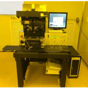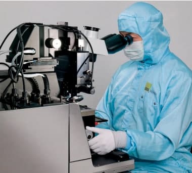
Mask Aligner MJB4
Easy to use and compact in size the SUSS MicroTec MJB4 represents the perfect system for laboratories and small volume production. As an inexpensive photolithography solution the MJB4 has set industry standards specifically for processing of small substrates and pieces up to 100 mm. Equipped with a reliable, high precision mask alignment and high resolution printing capability in the submicron range the MJB4 demonstrates a performance unsurpassed by any comparable machine.
- Description
- Additional information
Description
HIGHLIGHTS
The universal optics option (UV 250 / 300 / 400) for fast switching between different wavelengths
Fast and accurate alignment with SUSS Singlefield or Splitfield Microscope
SUSS MO Exposure Optics (MOEO) for excellent light uniformity, customized illumination and source mask optimization
High resolution printing down to 0.5µm
Wafer and substrate handling up to 100 mm
Upgradable with a UV nanoimprint lithography toolkit
Optional UV-LED light source
| Wafer Size | 1 up to 100 mm / 4″” (round) |
| Max. Substrate Size | 100 x 100 mm |
| Min. Pieces | 5 x 5 mm |
| Wafer Thickness | up to 4 mm |
| Mask Size | standard 2″” x 2″” up to 5″” x 5″” (SEMI) |
| Mask Thickness | up to 4.8 mm / 190 mil |
| EXPOSURE MODES | |
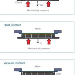
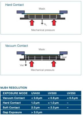
| Contact: soft, hard, vacuum, soft vacuum | |
| Vacuum contact | adjustable to 200 mbar abs |
| Gap exposure, | adjustable gap 10 – 50 µm |
| Flood exposure, split exposure | |
| Lamp control modes: constant power, constant intensity | |
| ALIGNMENT METHODS | |
| Top Side Alignment (TSA) Accuracy | < 0.5 µm (with SUSS recommended wafer targets) |
| Transmitted Infrared Alignment (IR) Accuracy | < 5 µm (2 µm under special process conditions) |
| Alignment Gap | 10 – 50 µm |
| ALIGNMENT STAGE | |
| MA Movement Range | X: ± 5 mm Y: ± 5 mm Theta: ± 5° |
| Mechanical Resolution | X, Y: 0.1 µm Theta: 4 x 10⁻⁵° |
| Topside Microscope (TSA) | |
| Movement Range | X: ± 40 mm |
| Y: + 30 – 50 mm | |
| Theta: ± 4° | |
| PHYSICAL DIMENSIONS | Width x Depth x Height: 605 x 810 mmx 660 mm |
| Weight up to 130 kg (290 kg with antivibration table) |
| EASY AND QUICK CHANGEOVER MJB4 allows for extremely quick changeover between different wafer sizes. Only chuck and maskholder need to be exchanged, which are easy accessible to the operator. Trained operators can do the wafer size changeover in less than five minutes. |
| EASY SOFTWARE With its ergonomic operation and its touch panel based user interface the MJB4 is very easy to operate and only requires minimum operator training. |
| SMALL FOOTPRINT In the MJB4, maximum functionality is packaged into minimal space. With a footprint of less than 0.5 m2 , the MJB4 requires only minimum cleanroom space. |
| TOP SIDE ALIGNMENT (TSA) Where lithographic processes require the alignment of structures on only one side of the device wafer (e.g. RDL, micro-bumping and similar techniques), top-side alignment is used to align the fiducials on the mask with those of the wafer. Depending on the substrate properties, this can be achieved either using stored position data for the wafer or through live image alignment, as with the DirectAlign® system invented by SUSS MicroTec. Mask aligner for the highest level of alignment precision Clear and stable pattern recognition even under poor contrast conditions |
| INFRARED ALIGNMENT Infrared Alignment Multilayer wafer stacks are used in a number of structuring processes. The alignment marks that are normally embedded between the layers can be identified and aligned via infrared (IR) illumination. This requires the use of materials that are transparent for IR light, such as undoped silicon, III-V semiconductors (e.g. GaAs) and adhesives for temporary bonding and debonding techniques. The SUSS equipment can be optionally equipped with powerful IR light sources and high-performance camera systems, ensuring optimal IR availability. |
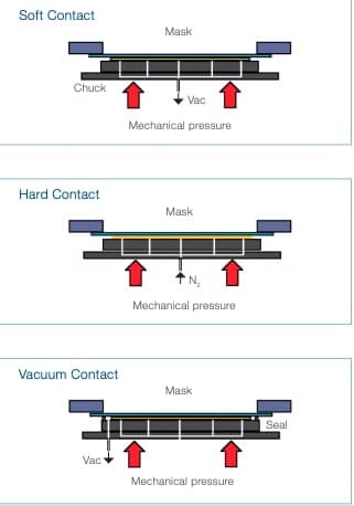
| EXPOSURE Soft contact:The lower the exposure gap from mask to wafer, the higher the resolution. In soft contact mode, the wafer is brought into contact with the mask and is fixed onto the chuck with vacuum. Hard contact: The lower the exposure gap from mask to wafer, the higher the resolution. In soft contact mode, the wafer is brought into contact with the mask and is fixed onto the chuck with vacuum. Vacuum contact: In this mode, a vacuum is drawn between mask and substrate during exposure. This results in a high resolution of < 0.8 µm. |
| EXPOSURE OPTICS HR and LGO optics: The large gap optics (LGO) optics is optimized for thick resist processes with large exposure gaps and 3D lithography, offering a resolution down to 5μm. The high resolution optics (HR) is apt for contact and close proximity lithography with structures down to 3μm at 20μm exposure gap. For processes with high dose requirements on 150 mm wafers the exceptionally high intensity of the W150 HR optics facilitates high throughput. Diffraction-Reducing Optics: Diffraction-reducing exposure optics are designed to compensate for diffraction effects in both contact and proximity lithography. Instead of using a plane wave as in other proximity lithography tools, it provides an angular spectrum of planar light waves to reduce diffraction effects. The selection of a proper angular spectrum improves structure resolution in the resist. |
| UV-LED LIGHT SOURCE The optional UV-LED light source concept of the MJB4 is highly efficient – UV-LED light sources reach many times the service life of conventional mercury vapor lamps. Moreover, they no longer need to warm up and cool down since the LED is only switched on during exposure. These factors significantly contribute to comparatively low energy consumption. |
| WEDGE ERROR COMPENSATION (WEC) SUSS mask aligners are equipped with an enhanced WEC head system providing additional functionality. By direct and instant gap measurement during the stacking process, the parallelism between substrate and substrate, mask or stamp is reached with micrometric precision. This enables significant improvements in resolution compared to mechanical gap measurement. |
 |  |
| Power Supply | |
| Power Voltage: | AC 230 V ± 10 % |
| Frequency: 50 – 60 Hz | 50 – 60 Hz |
| Vacuum: | – 0.8 bar |
| Compressed Air: | 5.5 bar |
| Nitrogen: | 1.5 bar |
| antivibration table | |
| Clean room: Class 1000 |
| The MJB4 Mask Aligner from SUSS MicroTec is the perfect system for research institutes, universities and small volume production. Easy to use and compact in size, the SUSS MJB4 has set industry standards specifically for processing of small wafers /substrates or pieces and offers an ideal and cost-effective solution for customers with limited budgets. |
| The MJB4 is used for lithography of LED |
| Microfluidics device |
| Piezo motor for MEMS applications |
| Structures with steep sidewalls manufactured in 100 to 200 µm thick SU8 resist |
| Reliable submicron patterning with MJB4 diffraction reducing optics. 0.6 µm resolution at 0.8 µm resist thickness |
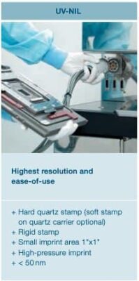
| UV-NIL (ultraviolet nano-imprint lithography) is a low-costsolution for replicating structures in small areas with resolution as low as a few nanometers. With UV-NIL technology, a rigid quartz stamp transfers structures onto a UV-sensitive resist coating on the substrate. Afterwards the material cures under exposure to UV light. The mask aligner platform comprehensively supports the printing process with wedge error compensation that enables precise levelling of the substrate to the stamp, which is fundamental to imprint uniformity. Stamp and substrate can also be accurately aligned. The setup allows for precise control of all crucial process parameters such as pressure, distance and speed making the tool extremely versatile and ideal for research and development. Additional tooling is also suited to producing in-house low-cost test stamps with sub-micrometric resolution. UV-NIL technology by SUSS MicroTec delivers a valuable solution for developing of next-generation semiconductor, MEMS / NEMS and opto-electronic technology and is the ideal starter kit for Research. + Easy handling, especially suited to university environment + Alignment in submicron resolution + High leveling precision for good residual layer uniformity + Control of printing parameters via recipe editor + Long-life quartz stamp provides high resolution |
| Mask holder | for Mask 2×2, 5×5 “ |
| Wafer Chuck | for wafer from 1″ to 4″ |
| Ojective | “Magnification is selectable Single Objective UMPL FL 5X/0.15 Single Objective UMPL FL 10X/0.30” |
| VACUUM PUMP | VACUUM PUMP (DOUBLE MEMBRANE) 220V/50HZ CPL Part no. G206200 |
| SUSS UV LIGHT MEASURING PROBE 365/405NM for UV OPTOMETER | |
| Lab Simulation Software | A simulation of lithographic processes makes the selection of optimal settings for process parameters possible without long-winded trial and error sessions. The multi-functional simulation software of lithographic processes “Lab”, which SUSS MicroTec distributes together with the supplier, GenISys, first and foremost allows the operator better process control. It offers all the required simulation functionality for an integrated design and process development, as well as verification and optimization. At the same time it covers all the process steps from illumination shaping and mask layout optimization up to photo resist processing. Additionally, modern 3D simulation functions improve the model visualizations. |
| Nanoimprint Lithography | Imprint lithography represents a cost-effective and highly reliable means of transferring three-dimensional nano- or micro-scale patterns onto a wide variety of substrates. For the imprint, a stamp is brought into contact with a photosensitive material on the substrate. The photoresist fills out the three-dimensional pattern of the stamp and then solidifies under UV light. Parameters such as pattern topography, structure resolution and aspect ratio have a considerable influence on the process quality. |
| Mask aligner | |
| Integrated software Software easy to use, user interface friendly Mask and wafer alignment control, simulator included Creating and saving Recipe and parameters Automatic warning when there is an error |
Additional information
| Manufacturer | Suss |
|---|---|
| Origin | Germany |
| Type | Manual |