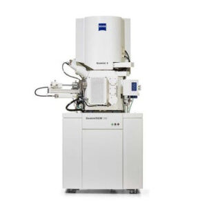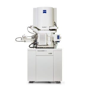
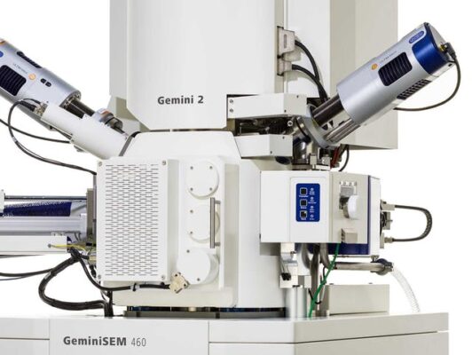
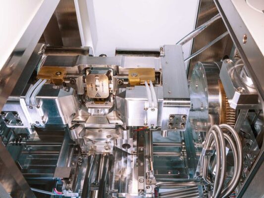
ZEISS GeminiSEM 460
ZEISS GeminiSEM 460 is made for the most exacting analytical tasks. Characterize your specimens comprehensively and efficient by using multiple detectors simultaneously.
- Description
- Additional information
Description
HIGHLIGHTS
Utilize High Resolution and High Current
+ GeminiSEM 460 is made for your most exacting analytical tasks and enables efficient analysis and unattended workflows.
+ Perform high-resolution imaging and analytics rapidly
+ Characterize any specimen comprehensively by using multiple detectors in parallel.
Customized, Automated Workflows
+ With such powerful analytics at hand workflow automation becomes key. Create and configure automated experiments of your own with the Python scripting API from ZEISS.
+ Modify experiments and customize the outcome to your own requirements.
+ Make the most of STEM tomography: combine automated fly.
Your Pathway to Even More Possibilities
+ Expand your analytical capabilities across materials and life sciences with exceptionally high, tunable current density, even at low kV – based on the Gemini 2 design.
+ All GeminiSEMs are plugged into the ZEISS ZEN core ecosystem giving you access to ZEN Connect, ZEN Intellesis and ZEN’s analytical modules providing reporting and GxP workflows
| – Resolution: | 0.6 nm @ 30 kV (STEM), 0.7 nm @ 15 kV, 1.0 nm @ 1 kV / 500 V TD, 1.1 nm @ 1 kV / 500 V, 1.5 nm @ 200 V. |
| – Analytical Resolution: | 2.0 nm @ 15 kV, 5 nA, WD 8.5 mm |
| – Inlens BSE Resolution: | 1.2 nm @ 1 kV |
| – Resolution in NanoVP mode (30 Pa): | 1.4 nm @ 3 kV, 1.0 nm @ 15 kV |
| – Acceleration Voltage: | 0.02 – 30 kV |
| – Probe Current: | 3 pA – 40 nA (100 nA or 300 nA configuration also available) |
| – Maximum field of view in high resolution mode: | 5 mm at 5 kV and WD = 8.5 mm |
| – Magnification: | 8 – 2,000,000 |
| – Electron Emitter: | Thermal field emission type, stability better than 0.2 %/h |
| – Detectors available with basic configuration: | Inlens Secondary Electron detector, Everhart Thornley Secondary Electron detector |
| – Selected Optional Detectors: | High efficiency VPSE detector, Cascade current detector (C2D), Annular solid state backscattered detector (aBSD), Angular selective backscattered detector (AsB4), Annular STEM detector (aSTEM4). |
| – Store Resolution: | Up to 32k × 24k pixels |
| – Specimen Stage: | |
| + 5-axes motorized eucentric specimen stage | |
| + X = 130 mm; Y = 130 mm | |
| + X = 130 mm; Y = 130 mm | |
| + T = -4º to 70º | |
| + R = 360º (continuous) | |
| + Specimen size: up to 179 mm in diameter for the full stage travel range of 130 mm. | |
| + Additional stage options available on request |
Conduct rapid analysis and achieve high current and high resolution simultaneously.
Configure your instrument tailored to your needs thanks to the versatile chamber.
Turn your GeminiSEM 460 into an in situ lab.
Updating…
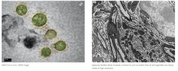
Materials Sciences
+ Nanoscience & Nanomaterials
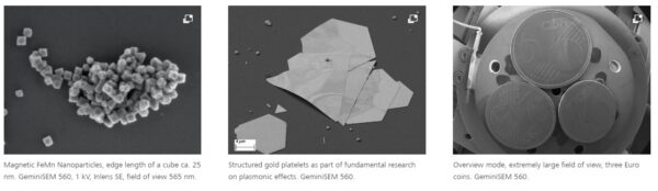
+ Energy Materials
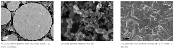
+ Bio-inspired Materials, Polymers and Catalysts
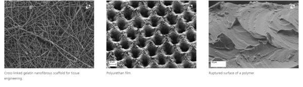
Industry
+ Microscopy Solutions for Industry
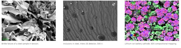
Electronics and Semiconductor
+ Semiconductor Device Design and Failure Analysis
Life Sciences
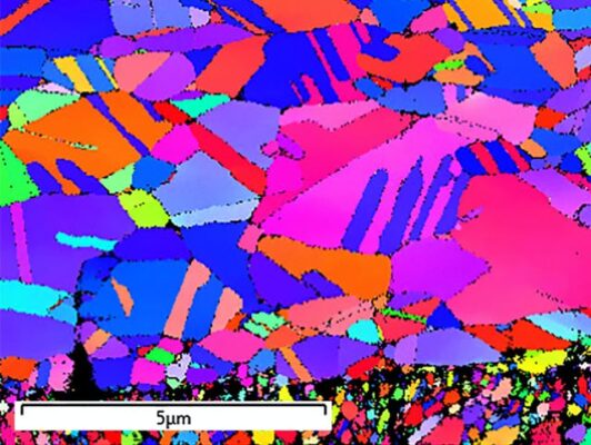
+ Characterization of topology
+ Imaging sensitive, non-conductive, outgassing, or low contrast samples
+ Visualizing the ultrastructure of cells, tissues etc. at high resolutions
+ Imaging very large areas such as serial sections or block faces
Updating…
| ZEN Connect: Module to organize and align image data in a correlative workspace |
| ZEN Connect 2D Add on: Module for an automated correlative 2D workflow that overlays data of light microscopes and SEMs |
| ZEN Automated Imaging: SEM image acqusition within the workspace of ZEN Connect to set up regions using predefined protocols |
| ZEN Intellesis: Module for machine learning based image segmentation |
| ZEN Data Storage: Central database accessible from any microscope or analysis workstation |
| 3DSM (3 dimensional surface modeling): Module for real time three dimensional surface modeling |
Additional information
| Manufacturer | Zeiss |
|---|---|
| Origin | Germany |
| Type | Semiautomatic |