")
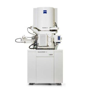
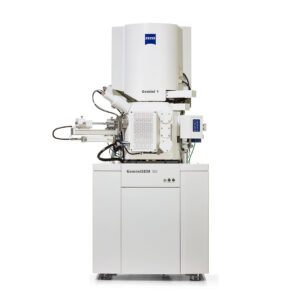
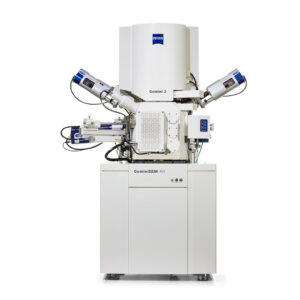
ZEISS Sigma 500
The ZEISS Sigma family combines field emission SEM (FE-SEM) technology with an excellent user experience. Structure your imaging and analysis routines and increase productivity with Sigma’s intuitive 4-step workflow. You’ll capture more data, faster than ever before. Choose from a variety of detector options to tailor Sigma precisely to your applications: you can image particles, surfaces, nanostructures, thin films, coatings and layers.
- Description
- Additional information
Description
HIGHLIGHTS
Flexible Detection for Clear Images
+ Tailor Sigma to your needs using the latest detection technology and characterize all of your samples.
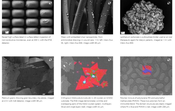
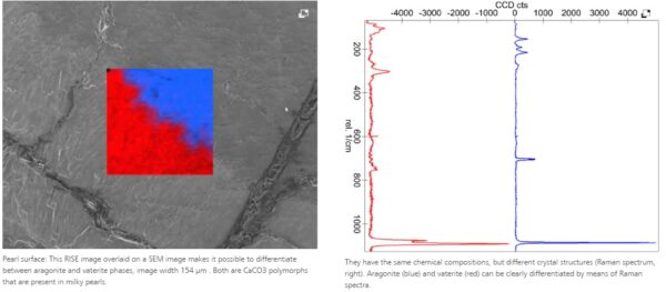
+ Characterize composition, crystallography and surface topography with the annular backscatter detector (aBSD). It delivers excellent low kV images under all vacuum conditions.
+ Benefit from improved sensitivity, increased signal-to-noise ratio, and more speed.
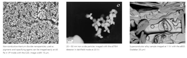
+ Enjoy a new generation of secondary electron (SE) detectors. Benefit from the C2D and VPSE detectors of Sigma in variable pressure mode: working at low vacuum, you can expect crisp images with up to 85% more contrast.
Automate and Speed up Your Workflow
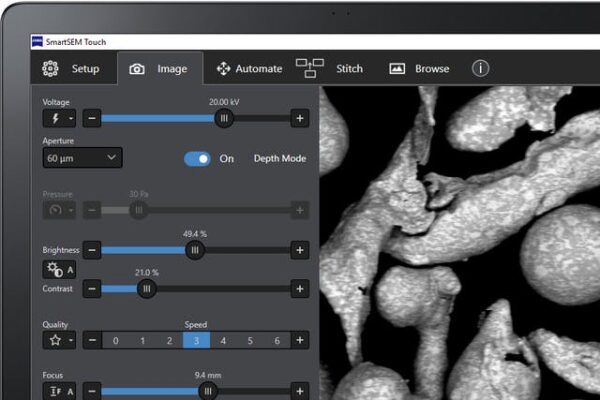
+ A 4-step workflow lets you control all the functionality of your Sigma. Benefit from fast time-to-image and save time on training – especially in a multi-user environment.
+ First, navigate your sample and then set optimal imaging conditions.
+ Next, automatically acquire images across multiple samples utilizing regions of interest (ROIs). + Finally use the workflow’s last step for contextual visualization of your results.
+ Finally, SmartSEM Touch collects and presents your data as an interactive map so you can understand your sample completely.
Perform Advanced Analytical Microscopy
+ Combine scanning electron microscopy and elemental analytics: the best-in-class EDS geometry of Sigma increases your analytical productivity, especially on beam sensitive samples.
+ Get analytical data at half the probe current and twice the speed.
+ Achieve complete, shadow-free analytics in your FE-SEM. Profit from using a short analytical working distance of 8.5 mm and a take-off angle of 35°.
| – Electron Source: Schottky Thermal Field Emitter | Schottky Thermal Field Emitter |
| – Resolution* at 30 kV (STEM): | 1.0 nm |
| – Resolution* at 15 kV: | 1.0 nm |
| – Resolution* at 1 kV: | 1.6 nm |
| – Resolution* at 30 kV (VP Mode): | 2.0 nm |
| – Backscatter Detector (BSD): | aBSD / HDBSD |
| – Maximum Scan Speed: | 50 ns/pixel |
| – Accelerating Voltage: | 0.02 – 30 kV |
| – Magnification: | 10× – 1,000,000× |
| – Probe Current: | 3 pA – 20 nA (100 nA optional) |
| – Image Framestore: | 32 k × 24 k pixels |
| – Ports: | 10 |
| – EDS Ports: | 2 (1 dedicated port) |
| Vacuum Modes: | |
| – High Vacuum: | Yes |
| – Variable Pressure: | 10-133 Pa |
| – Stage Type: | 5 axis compucentric stage |
| – Stage travel X: | 125 mm |
| – Stage travel Y: | 125 mm |
| – Stage travel Z: | 50 mm |
| – Stage travel T: | -10 to +90 degrees |
| – Stage travel R: | 360° Continuous |
Leverage comprehensive sample characterization with two unique Inlens detectors configured in parallel.
Configure your instrument tailored to your needs thanks to the versatile chamber.
Perform multimodal experiments with ZEN Connect and understand your specimens completely.
Updating…
Materials Research
– High resolution imaging and analysis of novel nano-materials
– Analysis of coatings and thin films
– Characterization of various forms of carbon and other 2D materials
– Imaging, analysis and differentiation of polymer materials
– Performing battery research to understand aging effects and quality improvements
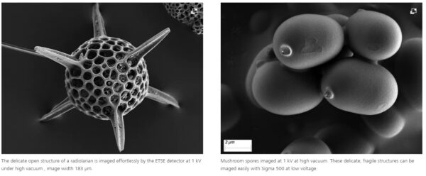
Life Sciences
– High resolution imaging and high throughput analysis of cryo-fixed
biological samples
– Research on organic specimens like teeth, bone, collagen-containing
bio-polymers like hair
Geoscience and Mineralogy
– Complete characterization of minerals and rocks
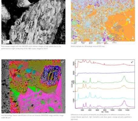
Natural Resources
– Fast, accurate investigation of mineralogic core samples
– Achieving high throughput in central laboratories
– Correlative classification for phase distinction
Industrial Applications
– Failure analysis of materials and manufactured components
– Imaging and analysis of steels and metals
– Inspection of medical devices
– Characterization of semiconductor and electronic devices in process control and diagnostics
– Getting a chemical fingerprint of semiconductor materials and devices by identifying their unique vibrational and rotational energy level structure
Updating…
– ZEISS SmartSEM Touch – Get more Hands on Deck
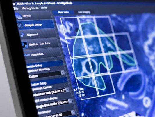
– ZEISS Atlas 5 – Master Your Multi-scale Challenge
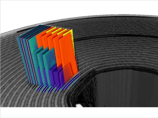
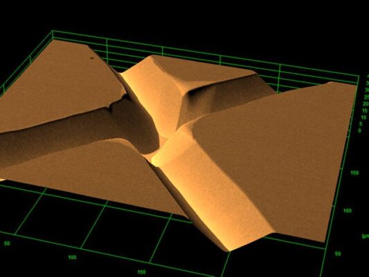
– 3D Surface Modelling – 3DSM
– Visualization and Analysis Software ZEISS recommends Dragonfly Pro from Object Research Systems (ORS)
Additional information
| Manufacturer | Zeiss |
|---|---|
| Origin | Germany |
| Type | Semiautomatic |