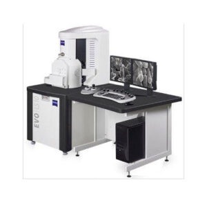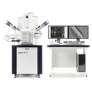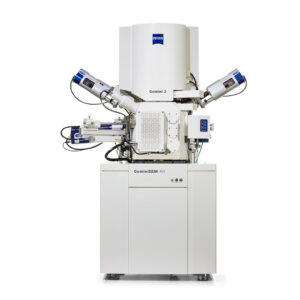
ZEISS Sigma 300
The ZEISS Sigma family combines field emission SEM (FE-SEM) technology with an excellent user experience. Structure your imaging and analysis routines and increase productivity with Sigma’s intuitive 4-step workflow. You’ll capture more data, faster than ever before. Choose from a variety of detector options to tailor Sigma precisely to your applications: you can image particles, surfaces, nanostructures, thin films, coatings and layers.
With the Sigma family you enter the world of hig h-end imaging: Sigma 300 delivers excellence in price and performance while Sigma 500’s best-in-class EDS geometry delivers superb analytical performance
- Description
- Additional information
Description
HIGHLIGHTS
Flexible Detection for Clear Images
+ Tailor Sigma to your needs using the latest detection technology and characterize all of your samples.
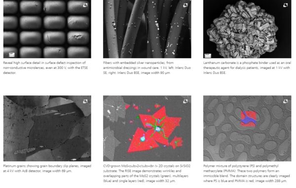
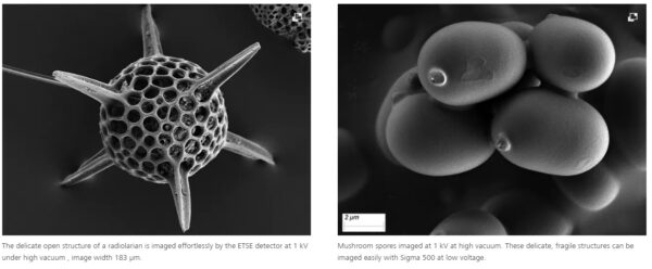
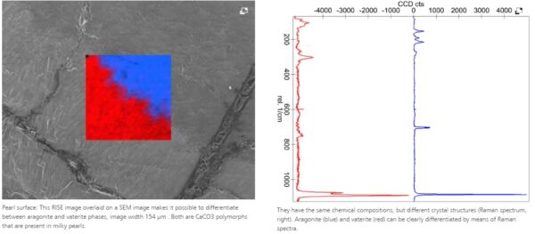
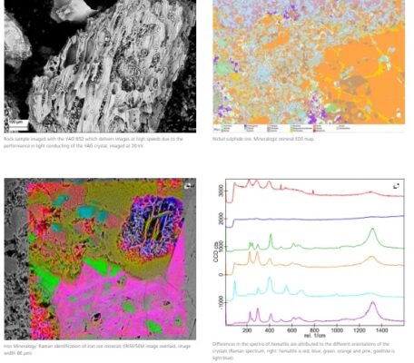
+ Characterize composition, crystallography and surface topography with the annular backscatter detector (aBSD). It delivers excellent low kV images under all vacuum conditions.
+ Benefit from improved sensitivity, increased signal-to-noise ratio, and more speed.
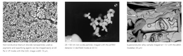
+ Enjoy a new generation of secondary electron (SE) detectors. Benefit from the C2D and VPSE detectors of Sigma in variable pressure mode: working at low vacuum, you can expect crisp images with up to 85% more contrast.
Automate and Speed up Your Workflow
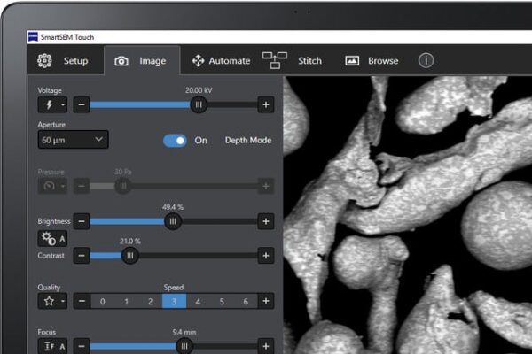
+ A 4-step workflow lets you control all the functionality of your Sigma. Benefit from fast time-to-image and save time on training – especially in a multi-user environment.
+ First, navigate your sample and then set optimal imaging conditions.
+ Next, automatically acquire images across multiple samples utilizing regions of interest (ROIs). + Finally use the workflow’s last step for contextual visualization of your results.
+ Finally, SmartSEM Touch collects and presents your data as an interactive map so you can understand your sample completely.
Perform Advanced Analytical Microscopy
+ Combine scanning electron microscopy and elemental analytics: the best-in-class EDS geometry of Sigma increases your analytical productivity, especially on beam sensitive samples.
+ Get analytical data at half the probe current and twice the speed.
+ Achieve complete, shadow-free analytics in your FE-SEM. Profit from using a short analytical working distance of 8.5 mm and a take-off angle of 35°.
| – Electron Source: Schottky Thermal Field Emitter | Schottky Thermal Field Emitter |
| – Resolution* at 30 kV (STEM): | 1.0 nm |
| – Resolution* at 15 kV: | 1.0 nm |
| – Resolution* at 1 kV: | 1.6 nm |
| – Resolution* at 30 kV (VP Mode): | 2.0 nm |
| – Backscatter Detector (BSD): | aBSD / HDBSD |
| – Maximum Scan Speed: | 50 ns/pixel |
| – Accelerating Voltage: | 0.02 – 30 kV |
| – Magnification: | 10× – 1,000,000× |
| – Probe Current: | 3 pA – 20 nA (100 nA optional) |
| – Image Framestore: | 32 k × 24 k pixels |
| – Ports: | 10 |
| – EDS Ports: | 2 (1 dedicated port) |
| Vacuum Modes: | |
| – High Vacuum: | Yes |
| – Variable Pressure: | 10-133 Pa |
| – Stage Type: | 5 axis compucentric stage |
| – Stage travel X: | 125 mm |
| – Stage travel Y: | 125 mm |
| – Stage travel Z: | 50 mm |
| – Stage travel T: | -10 to +90 degrees |
| – Stage travel R: | 360° Continuous |
Updating…
Materials Research
– High resolution imaging and analysis of novel nano-materials
– Analysis of coatings and thin films
– Characterization of various forms of carbon and other 2D materials
– Imaging, analysis and differentiation of polymer materials
– Performing battery research to understand aging effects and quality improvements
Life Sciences
– High resolution imaging and high throughput analysis of cryo-fixed
biological samples
– Research on organic specimens like teeth, bone, collagen-containing
bio-polymers like hair
Geoscience and Mineralogy
– Complete characterization of minerals and rocks
Natural Resources
– Fast, accurate investigation of mineralogic core samples
– Achieving high throughput in central laboratories
– Correlative classification for phase distinction
Industrial Applications
– Failure analysis of materials and manufactured components
– Imaging and analysis of steels and metals
– Inspection of medical devices
– Characterization of semiconductor and electronic devices in process control and diagnostics
– Getting a chemical fingerprint of semiconductor materials and devices by identifying their unique vibrational and rotational energy level structure
Updating…
– ZEISS SmartSEM Touch – Get more Hands on Deck
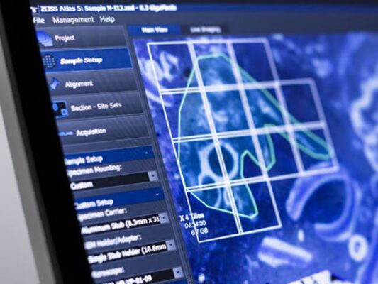
– ZEISS Atlas 5 – Master Your Multi-scale Challenge
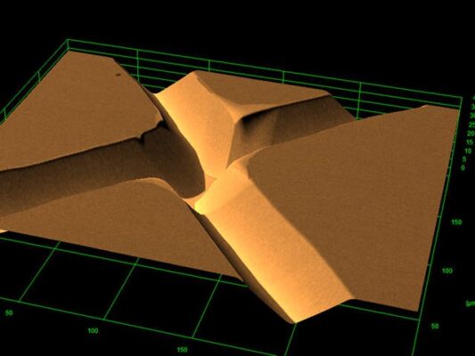
– 3D Surface Modelling – 3DSM
– Visualization and Analysis Software ZEISS recommends Dragonfly Pro from Object Research Systems (ORS)
Additional information
| Manufacturer | Zeiss |
|---|---|
| Origin | Germany |
| Type | Manual |