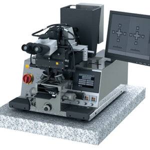
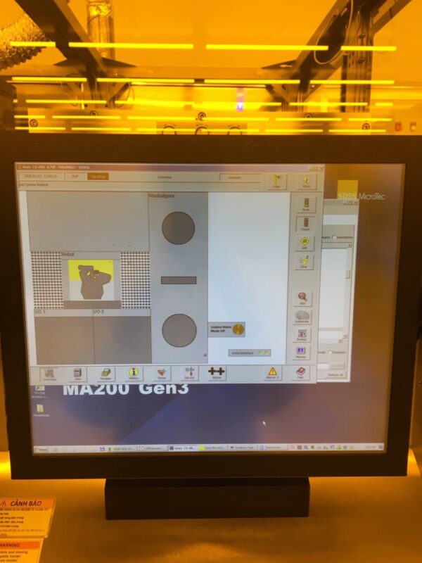
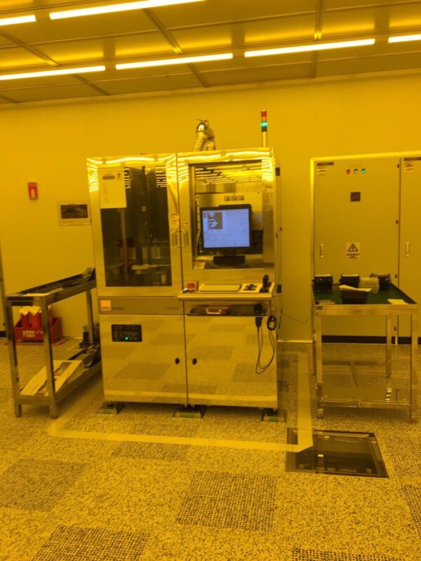
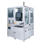
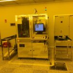

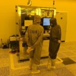
MA200 gen3
- Mô tả
Mô tả
HIGHLIGHTS
Leading process stability
Superior reliability
Unmatched throughput for thick materials
Process flexibility for a multitude of applications
Over seventy years of industry and process experience
| EXPOSURE SYSTEM | |
| Resolution HR LGO | 3 μm (20 μm proximity) 7μm (100 μm gap) 10 μm (150 μm gap) |
| Accuracy in Constant Dose exposure system | <1% |
| Exposure mode | Vacuum contact, hard contact, soft contact, proximity, flood exposure |
| INTENSITY / UNIFORMITY* | |
| Optics Type (1000 W) | |
| UV400 HR W200 | 365 nm/36 mW/cm2 |
| W200 Broadband | 69 mW/cm2/ < 3.5 % |
| UV400 HR LGO | 365 nm/16 mW/cm2 |
| W200 Broadband | 33 mW/cm2/ < 3.5 % |
| UV400 MO | 365 nm/31 mW/cm2 |
| HR-IFP W200 | 60 mW/cm2/ < 2.5 % |
| UV400 | 365 nm/75 mW/cm2 |
| HR W150 | 170 mW/cm2/ < 3.5 % |
| Optics Type (UV-LED) | |
| UV400 MO | 365 nm/25 mW/cm2 |
| HR-IFP W200 | 60 mW/cm2/ < 2.5 % |
| ALIGNMENT SYSTEM | |
| Alignment Accuracy | 0.5 μm / 3 IJ (TSA, AutoAL, DirectAlign) 1 μm / 3 IJ (TSA, AutoAL) 1 μm / 3 IJ (BSA, AutoAL) |
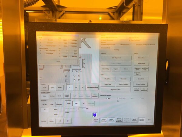
| Pattern Recognition | Cognex (CNL, PatMax) |
| Run-Out Compensation | ThermAlign chuck (optional) |
| Large Clear Field Alignment | 1 μm |
| Prealignment Accuracy | < 50 μm |
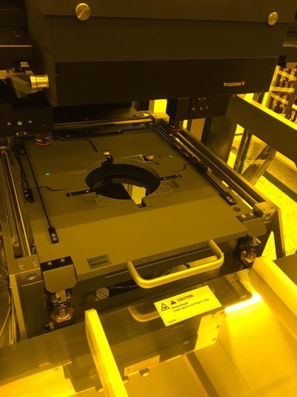
| WAFER HANDLING | |
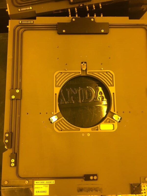
| Wafer Size | 2” -200 mm, round or square |
| Allowable Wafer Warpage | 1 mm |
| Perforated Wafers | Yes |
| Thin Wafers without Carrier (200 mm) | Thickness: down to 120 μm Max. warpage: 5 to 6 mm |
| Throughput | > 160 wph FM; > 130 wph AutoAL |
| Wafer Size Conversion | < 5 minutes |
| Height x Width x Depth | 2000 mm x 1509 mm x 1405 mm |
| TOP SIDE ALIGNMENT (TSA) Where lithographic processes require the alignment of structures on only one side of the device wafer (e.g. RDL, micro-bumping and similar techniques), top-side alignment is used to align the fiducials on the mask with those of the wafer. Depending on the substrate properties, this can be achieved either using stored position data for the wafer or through live image alignment, as with the DirectAlign® system invented by SUSS MicroTec. |
| BOTTON SIDE ALIGNMENT (BSA) Alignment of the structuring on the wafer back side with the structures on the front is required in processes in the field of MEMS, wafer-level packaging, 3D integration and imprint applications. Optical bottom-side alignment is normally used for this type of alignment. An integrated camera system detects the mask or stamp structures and the structures on the substrate back side, and aligns them with each other. The substrate position must be determined and stored prior to loading, since the substrate subsequently covers the mask target. This places specialized demands on the alignment system as a whole. |
| ENHANCING ALIGMENT PRECISION When stringent demands are made of overlay accuracy, the auto-alignment functionality of the standard system can be considerably extended. DirectAlign®, the SUSS MicroTec enhanced functionality for structure detection software, uses live images instead of patterns from an image memory system. The technology is based on the PatMax industry standard and achieves outstanding results. With the use of DirectAlign® on a SUSS mask aligner, an accuracy of 0.25 µm can be achieved. The use of enhanced alignment is recommended for challenging alignment processes with structures that are easily confused or restricted fields of view. |
| INFARED ALIGNMENT Multilayer wafer stacks are used in a number of structuring processes. The alignment marks that are normally embedded between the layers can be identified and aligned via infrared (IR) illumination. This requires the use of materials that are transparent for IR light, such as undoped silicon, III-V semiconductors (e.g. GaAs) and adhesives for temporary bonding and debonding techniques. The SUSS equipment can be optionally equipped with powerful IR light sources and high-performance camera systems, ensuring optimal IR availability. |
| PROXIMITY LITHOGRAPHY A mask with a certain structure is aligned with the wafer in very close proximity (thus “proximity” lithography). During exposure, the shadow cast by the mask structure is transferred to the wafer. The resulting exposure quality depends on both the precision with which the mask and wafer are spaced apart and the optical system used for exposure. Being fast and suited to flexible implementation, this method is regarded as the most cost-effective technique for producing microstructures down to 3 µm in size. With contact exposure, resolutions in the sub-micron range can be achieved. Typical areas of use include wafer-level chip-scale packaging, flip chip packaging, bumping, MEMS, LED and power devices. The systems are deployed in high-volume production, as well as in industrial research. The mask aligners supplied by SUSS MicroTec are based on proximity lithography. |
| SOFT CONTACT EXPOSURE The lower the exposure gap from mask to wafer, the higher the resolution. In soft contact mode, the wafer is brought into contact with the mask and is fixed onto the chuck with vacuum. |
| HARD CONTACT EXPOSURE In hard contact mode, the wafer is brought into direct contact with the mask, while positive nitrogen pressure is used to press the substrate against the mask. A resolution in the 1 micron range is possible in hard contact mode. |
| VACUUM CONTACT EXPOSURE In this mode, a vacuum is drawn between mask and substrate during exposure. This results in a high resolution of < 0.8 µm. |
| HR AND LGO OPTICS The large gap optics (LGO) optics is optimized for thick resist processes with large exposure gaps and 3D lithography, offering a resolution down to 5μm. The high resolution optics (HR) is apt for contact and close proximity lithography with structures down to 3μm at 20μm exposure gap. For processes with high dose requirements on 150 mm wafers the exceptionally high intensity of the W150 HR optics facilitates high throughput. |
| DIFFRACTION REDUCING OPTICS Diffraction-reducing exposure optics are designed to compensate for diffraction effects in both contact and proximity lithography. Instead of using a plane wave as in other proximity lithography tools, it provides an angular spectrum of planar light waves to reduce diffraction effects. The selection of a proper angular spectrum improves structure resolution in the resist. |
| MO EXPOSURE OPTIC MO Exposure Optics® is a unique illumination optics system specifically designed for SUSS mask aligners. It is based on microlens plates instead of macroscopic lens assemblies. A simple plug and play changeover allows a quick and easy changeover between different angular settings, including the functionality of both classical SUSS HR (High Resolution) and LGO (Large-Gap Optics) illumination optics. The telecentric illumination provided by MO Exposure Optics improves light uniformity and leads to a larger process window. Yield enhancements are produced as a result. MO Exposure Optics also decouples the exposure light from the lamp source, so small misalignments of the lamp do not affect light uniformity. A decoupled light source saves setup and maintenance time and guarantees uniform illumination conditions during the entire lifetime of the lamp. |
| UV-LED LIGHT SOURCE The new lamp house concept from SUSS MicroTec convinces with efficiency — UV-LED light sources reach many times the service life of conventional mercury vapor lamps. Moreover, they no longer need to warm up and cool down — the LED is only switched on during exposure. These factors significantly contribute to comparatively low energy consumption. In contrast with mercury vapor lamps, no cumbersome disposal of hazardous waste is required. The SUSS UV-LED lamp house features the latest in technology and therefore meets the growing demand for environmental sustainability and energy efficiency. Cost-effectiveness The use of an LED lamp house significantly affects the operating costs of a mask aligner. The service life of an LED exceeds that of conventional lamps many times over, thereby lowering costs generated by changing lamps. Downtimes, the acquisition of new lamps, adjustments and the disposal of old material have all become a thing of the past. Guaranteed process flexibility Compared to conventional mercury vapor lamps, LED light sources not only work more efficiently but are also much more flexible to use. The UV-LED lamp house generally covers the same spectral region as mercury vapor lamps. The difference is that the UV-LED can switch specific wavelengths on and off. This eliminates the need to optically filter the light outside of the lamp house. Wavelengths are regulated via a programmed recipe which fulfills specific process requirements without filter change or recalibration. When interacting with SUSS MicroTec’s special MO Exposure Optics, the LED lamp house provides for maximum flexibility in process design. |
| WEDGE ERROR COMPENSATION (WEC) SUSS mask aligners are equipped with an enhanced WEC head system providing additional functionality. By direct and instant gap measurement during the stacking process, the parallelism between substrate and substrate, mask or stamp is reached with micrometric precision. This enables significant improvements in resolution compared to mechanical gap measurement. |
| AUTO ALIGNMENT Auto-alignment is based on a motorized alignment stage. The COGNEX® based pattern recognition software automatically recognizes wafer target locations and controls the movement of the alignment stage. Coupled with SUSS MicroTec‘s DirectAlign®, accuracy to 0.25 μm (0.5 µm for production tools) can be achieved. Auto-alignment enables highest repeatability of process results coupled with optimized throughput and minimum operator intervention. |
| AUTOMATIC FILTER CHANGE The mask aligner optionally offers an automatic filter exchange unit for up to four filters that are selected via process recipe. This removes the risk of operator errors and thus improves yield and effective throughput. |
| Power Voltage: | 400 VA, 3 Phase Y Power: 2800 VA, 50 Hz |
| Frequency: 50 – 60 Hz | 50 – 60 Hz |
| Vacuum: | – 0.8 bar |
| Compressed Air: | 5.5 bar |
| Nitrogen: | 1.5 bar |
| antivibration table |
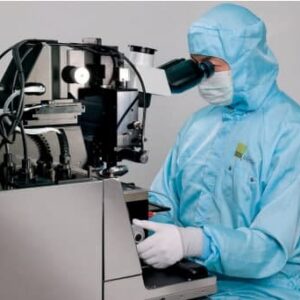
| Clean room: Class 1000 |
| MEMS With its high-intensity exposure optics the MA200 Gen3 efficiently processes the thick resist prevalent in MEMS application. Innovative features include specific process modules such as customized edge handling tooling, special tooling designed for warped wafer processing, and systems for infrared alignment and angular exposure for steep and perpendicular sidewalls. These features make the MA200 Gen3 an enabling lithography platform for the development and highvolume production of MEMS devices. |
| WAFER-LEVEL PACKAGING The MA200 Gen3 is geared to thick resist photolithography applications as used for advanced wafer-level packaging in general and advanced packaging processes like wafer bumping. High throughput combined with excellent overlay performance maximizes yield and ensures best possible cost of ownership. Equipped with additional features like warped wafer tooling, backside or infrared alignment, the MA200 Gen3 suits the process requirements of recently developed 3D packaging applications such as backside redistribution or TSV processes. |
| HB LEDs The MA200 platform is widely used in frontend and wafer-level packaging processes in HB LED manufacturing. Advanced pattern recognition ensures highly reliable and accurate alignment of blurred or low-contrast wafer targets. Fragile and warped wafer handling toolkits enable processing of compound semiconductors such as GaN or SiC. High throughput results combined with submicron alignment accuracy and special W150 optics with very high UV-light intensity make the MA200 Gen3 a highly efficient production system for manufacturing cost-sensitive devices like HB LED. |
| Mask holder | standard 2″ x 2″ up to 7″ x 7″ (SEMI) or up to 9″ x 9″ (SEMI) |
| Wafer Chuck | 1″ to 150 or 200 mm |
| Ojective | Magnification is selectable Single Objective UMPL FL 5X/0.15 Single Objective UMPL FL 10X/0.30 |
| Vacuum pump | VACUUM PUMP (DOUBLE MEMBRANE) 220V/50HZ CPL Part no. G206200 |
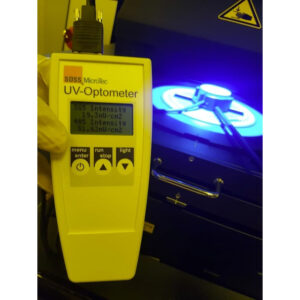
| Suss UV light measuring probe 365/405NM for UV OPTOMETER |
| Silicon wafer 4″ , 6 “ |
| UV- Led Lamp house |
| Optic type |
| ThermAlign | Overlay accuracy regularly suffers considerable degradation due to the thermal run-out between photomask and the wafer. The SUSS MicroTec compensation system ThermAlign® ensures a constant temperature on the wafer chuck and additionally provides a stabilizing influence on the mask temperature. ThermAlign® compensates for run-out effects by adapting the temperature to the process conditions. |
| Implementation with Dark Field Masks | Large clearfield alignment is used in dark field mask applications. These contain very small clearfields, which means the targets on the wafer are difficult to localize. The large clearfield method allows the mask to be moved out of the visual field and so the target on the wafer is localized without being obscured by the mask itself. |
| Error rate reduction | For the alignment of specific challenging process requirements SUSS MicroTec offers the enhanced alignment function package which significantly reduces the error rate based on redundancy. For situations where the alignment marks are damaged the system offers the option of defining replacement positions. Furthermore, it enables a two-stage final alignment process to be carried out which consists of an initial coarse alignment using guide marks followed by a fine alignment carried out using the same marks. The use of enhanced alignment is recommended for complex processes with easily confused structures, such as with advanced packaging, for example, or with restricted fields of view, such as with dark-field masks. |
| Exposure Gap Stabilization | With its intelligent gap setting system SUSS MicroTec offers an additional alignment stabilization and thereby ensures increased process reliability. The system measures the gap between carrier and photomask and automatically corrects any deviation from the set value. The control process ensures that wafers feed into the exposure only when their position is correct. Early detection of uncorrectable errors protects valuable customer materials. |
| LAB Simulation Software | A simulation of lithographic processes makes the selection of optimal settings for process parameters possible without long-winded trial and error sessions. The multi-functional simulation software of lithographic processes “Lab”, which SUSS MicroTec distributes together with the supplier, GenISys, first and foremost allows the operator better process control. It offers all the required simulation functionality for an integrated design and process development, as well as verification and optimization. At the same time it covers all the process steps from illumination shaping and mask layout optimization up to photo resist processing. Additionally, modern 3D simulation functions improve the model visualizations. The combination of MO Exposure Optics and the for SUSS optics custom-developed optical models in Lab facilitates customer-specific design optimization of the exposure filter plates, which in turn leads to an improvement in pattern fidelity. |
| Source-Mask Optimization | Combining optimization of mask layouts and the light source (source mask optimization), a procedure from projection lithography, makes it possible to reduce pattern inaccuracies due to illumination errors, processing artifacts and diffraction. A combined selection to match the exposure filter plates with the mask patterns (OPC = optical proximity correction) to customer specific requirements allows considerable expansion of the lithographic process functionality. A simulation platform permits modeling of process parameters such as mask patterns and illumination parameters. This facilitates the exposure and mask patterns to be set for specific production situations with a reduced experimental effort, and reduces illumination and process errors. Source mask optimization, together with SUSS MicroTecs customizable MO Exposure Optics® form an important contribution to improvement of process stability in mask aligner lithography. |
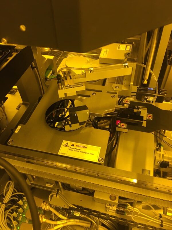
| Wafer Handling Toolings | Handling Fragile and Bent Substrates Handling wafers is the major challenge when automating production processes. In a production environment with high process change rates and therefore a large number of different substrates, for example in foundry production, the handling systems have to meet rapidly changing requirements. The reliability of the automatic handling has a direct effect on through-put and yield. SUSS mask aligners have a choice of flexibly interchangeable special tooling for handling the widest range of fragile, bent or warped substrates, and the tooling can be customized even further for particularly arduous production processes according to customer specifications. Handling of Thinned Wafers A special vacuum chuck supports ultra-thin wafers with thicknesses of less than 120 µm and down to 50 µm. Handling of Warped Wafers Bent and warped wafers are carefully pulled flat before alignment and exposure. Due to the variety of the parameters that affect it, an optimal tooling implementation requires adaptation for the specific substrate. Edge Handling A special carrier system protects the wafer, especially suitable for the protection of double-sided structures as for MEMS applications. |
| Automation | The mask aligner is designed for integration into a fab automation system compatible to the SECS-II/GEM interface standards. Level and details of the communication will be specified on basis of the SUSS MicroTec core software solution. |
| MA Soffware is intergrated | |
| Simulation of lithographic processes A simulation of lithographic processes makes the selection of optimal settings for process parameters possible without long-winded trial and error sessions. The multi-functional simulation software of lithographic processes “Lab”, which SUSS MicroTec distributes together with the supplier, GenISys, first and foremost allows the operator better process control. It offers all the required simulation functionality for an integrated design and process development, as well as verification and optimization. At the same time it covers all the process steps from illumination shaping and mask layout optimization up to photo resist processing. Additionally, modern 3D simulation functions improve the model visualizations. The combination of MO Exposure Optics and the for SUSS optics custom-developed optical models in Lab facilitates customer-specific design optimization of the exposure filter plates, which in turn leads to an improvement in pattern fidelity. Highlights Complete simulation of the mask aligner lithographic process Adjustable illumination parameters (collimation, spectral composition), custom-developed for all SUSS optics Fast and flexible visualization and quantitative predictions in 1, 2 and 3D |