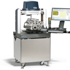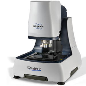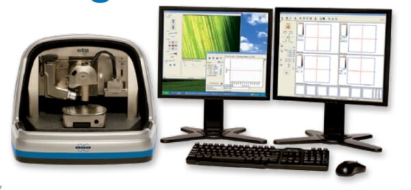
Atomic Force Microscope Dimension Edge
Dimension Edge™ incorporates Bruker’s PeakForce Tapping® technology to provide the highest levels of atomic force microscope (AFM) performance, functionality, and accessibility in its class. Based on the Dimension Icon platform, the Edge system has been designed from top to bottom to deliver the low drift and low noise necessary to achieve publication-ready data in minutes instead of hours, all at price points well below expectations for such performance. Integrated visual feedback and preconfigured settings enable expert-level results simply and consistently, making the most advanced large-sample AFM capabilities and techniques available to every facility and user.
- Mô tả
- Thông tin bổ sung
Mô tả
HIGHLIGHTS
Solutions for All Applications on Any Sample
• Open stage access accommodates wide variety of experiments and samples
• Optimized AFM modes and techniques meet needs of even advanced applications
• Built-in access to signal routing enables custom measurements
Accurate, High-Resolution Results Even Faster
• Linear workflow with visual feedback ensure optimized setup in shortest time
• Camera and stage provide best sample navigation and multi-site measurements
• Seamless transitions from survey to highest resolution deliver fast, accurate results
Best Value Closed-Loop Dimension AFM
• Proprietary sensor design achieves closed-loop accuracy with open-loop noise levels
• Reduced noise and drift bring small-sample imaging performance to large-sample AFM
• Microscope and electronics design enable high image fidelity at moderate cost
| – X-Y Scan Range | 90μm x 90μm typical, 85μm minimum |
| – Z Range | 10μm typical in imaging and force ramp modes, 9.5μm minimum |
| – Vertical Noise Floor | <50pm RMS in appropriate environment, typical imaging bandwidth (up to 625Hz) |
| – XY Position Sensor Noise Level (Closed Loop) | <0.5nm RMS typical imaging bandwidth (up to 625Hz) |
| – Z Position Sensor Noise Level (Closed Loop) | <0.2nm RMS typical imaging bandwidth (up to 625Hz) |
| – Sample/Size/Holder | 150mm vacuum chuck, 15mm thick; Up to 40mm thick with optional frame spacer |
| – Motorized Positioning Stage (X-Y axis) | 150mm x 150mm inspectable area; Programmable for multi-site measurements |
| – Microscope Optics | 5-megapixel digital camera; 180μm to 1465μm viewing area; Digital zoom and motorized focus |
| – Single Point Spectroscopy | Three-axis closed loop control for point-and-shoot positioning and ramping; Spring constant calibration with built-in thermal tune |
| – Sample Temperature Control | -35 to +250°C with optional heater/cooler accessory; Includes gas purging capability |
Closed-Loop Accuracy
At the heart of this system’s capabilities is Bruker’s renowned closed-loop scanner. Incorporating temperature-compensating position sensors and driven by modular, low-noise control electronics, this tip-scanning component reduces closed-loop positioning noise levels to the length scale of a single chemical bond.
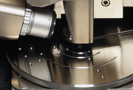
Large Sample Stage
The Dimension Edge sample stage is not only motorized and programmable for efficient multi-site measurements, but it also lets you fit more types of samples directly under the AFM scanner with less preparation time. The physically open access to the probe-sample junction enables more direct investigation of geometrically challenging device structures, as well as the attachment of electrical connections or other custom experiment accessories.
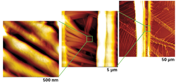
Automatic Image Optimization
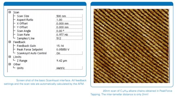
Edge uses “”intelligent”” algorithms to automatically and continuously monitor image quality and make the appropriate parameter adjustments. This frees researchers from the complex and tedious task of adjusting setpoints, feedback gains, and scan rates, making imaging as easy as simply selecting a scan area and scan size for almost any sample, in air or fluid.
AFM MODES
Expand Your Applications with AFM Modes
With an unrivalled suite of imaging modes available, Bruker has an AFM technique for every investigation.
Built on the backbone of core imaging modes—Contact Mode and Tapping Mode—Bruker offers AFM modes that allow users to probe their samples’ electrical, magnetic, or materials properties. Bruker’s innovative new PeakForce Tapping technology represents a new core imaging paradigm that has been incorporated into several modes, providing topographic, electrical, and mechanical properties data in parallel.
| – Vibration Isolation | Vibration isolation table or integrated vibration/acoustic isolation enclosure required |
| – Laser Classification | Class 2M |
Materials Science and Polymers
The Dimension Edge provides a full suite of nano-mechanical and nano-electrical modes to fulfill these needs, ranging from phase imaging and force spectroscopy to piezo-response force microscopy, conductive AFM, and Kelvin probe force microscopy. All modes benefit from the highest spatial resolution, to easily achieve atomic resolution.
Electrochemistry
Electrochemical AFM (ECAFM) maps surface changes in situ, while the sample is immersed in the electrolyte and under electrochemical control. Applications include fundamental electrochemistry studies, corrosion and Li battery development.
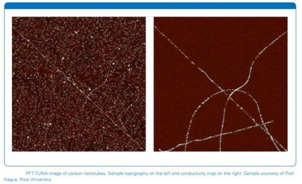
Nanoelectrical Measurement
AFM-based nanoscale electrical characterisation is an established technique in semiconductor R&D, where scanning capacitance provides maps of active carrier density and conductive AFM probes device connectivity and gate oxide breakdown characteristics.
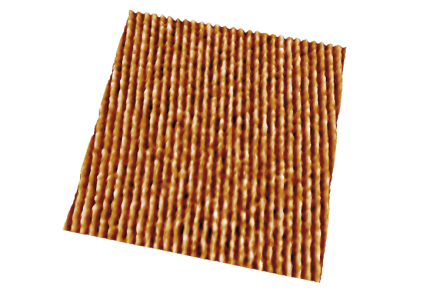
Patterned Sapphire Substrate
Patterned Sapphire Substrate (PSS) is used in LED manufacture, to enhance light output and efficiency. A PSS is typically a sapphire wafer, etched with a periodic pattern. Dimension Edge provides the metrology required to control the manufacture of PSS, including feature height, width and angle measurements, while also providing a full 3-D profile.
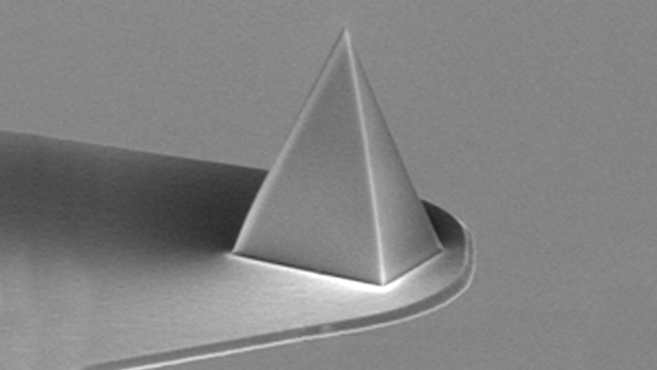
| -Bruker AFM Probes | Visit www.brukerAFMprobes.com to see our ocmprehensive listing of probes, including Bruker-exclusive ScanAsyst probes |
| – Optional AFM Modes: | Scanning Tunneling Microscopy, Conductive AFM, Tunneling AFM, Scanning Capacitance Microscopy, Surface Potential Microscopy, Piezoresponse Microscopy, Force Modulation Microscopy, Liquid Imaging, Thermal Analysis, Electrochemical AFM. |
PeakForce Tapping® and ScanAsyst®
The Dimension Edge™ Atomic Force Microscope (AFM) incorporates Bruker’s PeakForce Tapping™ technology to provide the highest levels of performa functionality, and accessibility in its class. Based on the Dimension Icon® platform, the Edge system has been designed from top to bottom to deliver the low drift and low noise necessary to achieve publication-ready data in minutes instead of hours, all at price points well below expectations for such performance. ScanAsyst® imaging, integrated visual feedback, and preconfigured settings enable expert-level results simply and consistently, making the most advanced large-sample atomic force microscopy capabilities and techniques available to every facility and user.
Thông tin bổ sung
| Hãng sản xuất | Bruker Nano |
|---|---|
| Xuất xứ | Đức |
| Loại | Thủ công |