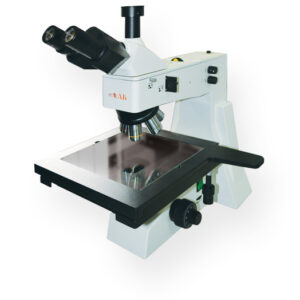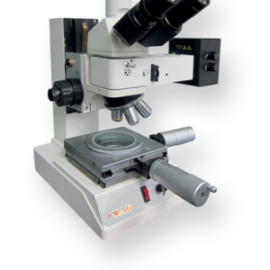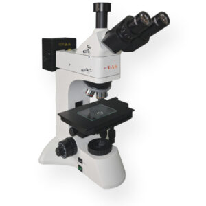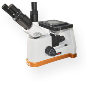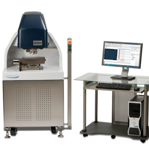
Stylus Profilometer DektakXT
The DektakXT® stylus profilometer features a revolutionary benchtop design that enables an unmatched repeatability of 4Å and up to 40% improvement in scanning speeds. This major milestone in stylus profiler performance is the culmination of over fifty years of Dektak® innovation and industry leadership. Through its combination of industry firsts, DektakXT delivers the ultimate in performance, ease of use, and value to enable better process monitoring from R&D to QC. The technological breakthroughs incorporated in DektakXT enable critical nanometer-level surface measurements for the microelectronics, semiconductor, solar, high-brightness LED, medical, and materials science industries.
- Mô tả
- Thông tin bổ sung
Mô tả
HIGHLIGHTS
• 4 angstrom repeatability
Delivers industry-leading accuracy.
• Single-arch design
Provides breakthrough scan stability.
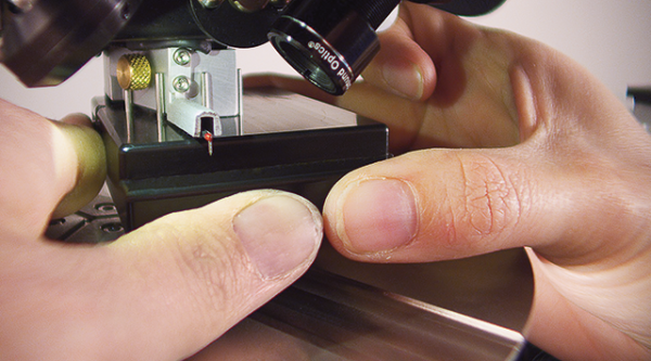
• Self-aligning stylus
Enables effortless tip exchange.
DektakXT Critical Results for Multiple Applications:
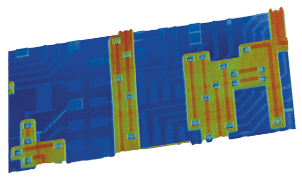
– Thin Film Inspection – Ensuring High Yield
– Surface Roughness Verification – Assuring Performance
– Solar Trace Analysis – Reducing Manufacturing costs
– Microfluidics – Verifying Design and Performance
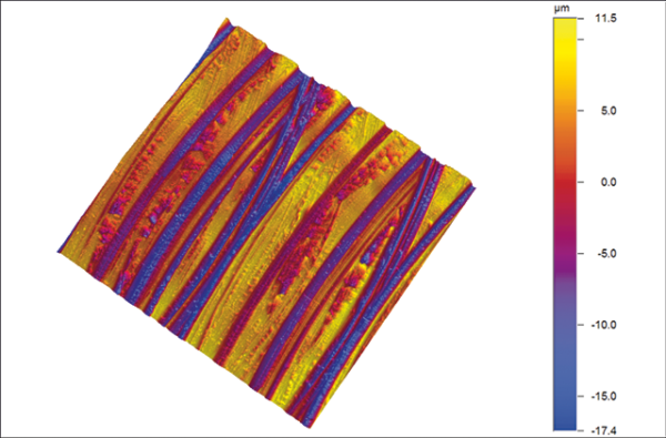
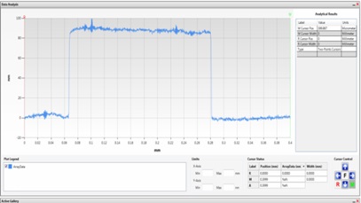
| – Two-dimensional surface profile measurement | |
| – Digital magnification, | 3.1Mpixel |
| – Vertical FOV: | 275 μm x 2.2 mm |
| – Sample X/Y Stage: | Manual 100 mm (4 in.) X/Y, manual leveling |
| – Sample R-Theta Stage: | Manual, continuous 360 degrees |
| – Integrated computer: | 64bit Desktop Computer |
| – Vibration isolation: | Isolation Pads (Kit of Four) |
| – Max. Sample Thickness: | 50 mm |
| – Max. Wafer Size: | 200 mm (8 in.) |
| – Step Height Repeatability: | 4Å, 1 sigma on steps ≤1 μm |
| – Vertical range (Z axis) : | 1 mm (0.039 in.) |
| – Vertical Resolution: | 1Å (@ 6.55 μm range) |
| – Dimensions | (550 mm L x 585 mm W x 445 mm H) 21.6” L x 23” W x 17.5” H |
| – Profiler Weight | 34 kg |
| – Enclosure Weight | 21.7 kg |
Accelerating Data Collection and Analysis
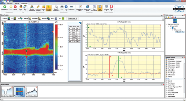
Utilizing a unique direct-drive scan stage, the DektakXT accelerates measurement scan times by 40% while maintaining industry-leading performance. Vision64, Bruker’s 64-bit parallel processing operation and analysis software, enables faster loading of 3D files and faster applications of filters and multiscan database analyses.
Delivering the Most Repeatable Measurements
Implementing a single-arch structure makes the DektakXT sturdier, which minimizes the effects of environmental noise. DektakXT’s upgraded “smart electronics” reduce temperature variations and employ modern processors that minimize error-inducing noise, allowing it to be an even more robust system capable of measuring <10nm step heights.
Perfecting Operation and Analysis
Bruker’s Vision64 software complements DektakXT’s innovative design by providing the most intuitive and streamlined visual user interface. The combination of intelligent architecture and customizable automation capabilities allow for fast and comprehensive data collection and analysis. Whether you’re using a recipe to perform routine analysis on single scans, or applying custom filters settings and calculations, DektakXT’s Data Analyzer displays current data while also revealing other possible analyses.
Making Things Easy
The DektakXT’s self-aligning stylus assembly allows the user to quickly and easily change stylus size while eliminating any potential mishaps during the process. Bruker offers the widest range of stylus sizes to accommodate nearly any application need.
Ensuring High Yield
DektakXT provides the ability to quickly and easily set up and run automated multi-site measurement routines to verify the precise thickness of thin films across the wafer surface with unmatched repeatability. This efficient monitoring can save valuable time and money by improving yields.
| – Power Supply | 100 – 240 VAC, 50 – 60 Hz |
| – Temperature | 20°-25°C (68°-77°F). |
| – Clean Room | Not required. (Class 1000 or better ) |
| – Relative Humidity | Less than 80% (non-condensing) |
| – Warm-up Time | 15 min. for maximum stability |
| – Vibration | Not to exceed 70 µg from 1 to 100 Hz on floor with flat noise spectrum. |
| – Vacuum (for optional vacuum chuck) | 457 – 635 mm Hg (18 – 25″) 0.61 – .85 BAR minimum constant vacuum for the system with one fitting for 3.175 mm (1/8″) OD tubing. Standard fitting is 3.175 mm (1/8″) slip connect. |
| – Clean, Dry Air (for optional vibration isolation pads) | 40 psi clean air maximum with 6.35 mm (1/4”) OD tubing |
| – Clean, Dry Air (for optional floor- model vibration isolation table) | 50 psi clean air for the system with one fitting for 6.35 mm (1/4″) OD tubing. Standard fitting is 6.35 mm (1/4”) slip connect. |
| – Acoustics | Not to exceed 60 dB(A) across the frequency spectrum. |
| Thinfilms Applications: – Microelectronics and Semiconductor devices – UV or hardness coatings on eye glasses or sun glasses. – Decorative coatings on faucets and fixtures (gold plating or other precious metals). – Pressure sensors for automotive or aerospace applications |
| Microelectronics Applications: – Monitoring deposition and etching processes – Microelectronics extend into aerospace, medical, automotive – Sensors in demanding environments – Rigid ceramics to flexible circuits. |
| Solar Applications: – Inspection of conductive streets – Monitoring deposition process of thin film – Thin film stress measurements |
| Film Stress Applications – Stress causes bowing or warping of substrate leading to de-lamination of layers, cracking or lithography problems – Stylus profilers perform long scans (up to 200mm) before and after deposition to compare wafer bow caused by thin film stress – Stylus profiler calculates tensile and compressive stress in MPa |
| Machined Surface Applications: – Medical application: Verification of hydroxyapatite growth on implant backside – Inspection of polished surfaces |
| MEMS Applications: – Measure large vertical features of sensitive materials (up to 1mm tall) – Low force measurement capability applies a light touch on sensitive materials to measure vertical steps and roughness without damaging the sample’s surface |
| +Low Force Capabilities |
| N-Lite+ low force sensor reduces minimum stylus force down to 0.03mg. |
| +X-Y- Theta Auto Stage: |
| Motorized/programmable X-Y sample positioning (150mm x 150mm X-Y translation) and motorized 360 degree theta rotation |
| +3D Scanning: |
| Enables 3D mapping of sample area with 1 micron minimum spacing between scan lines (with up to 200 3D map locations per program) and includes the exclusive Vision 3D analysis software. Requires XY-Auto stage option. |
| +Scan Stitching: |
| Enables the maximum scan length to be extended from the standard 55mm up to 150mm. Useful for stress measurements on larger wafers (Requires XY-Auto Stage). |
| +Ceramic Vacuum Chucks: |
| – 2 inch diameter to hold small or flexible samples – 6 inch square (designed for solar applications) |
| +Wafer Vacuum Chucks |
| – 2 and 3 inch wafer vacuum chuck with alignment pins – 4 and 6 inch wafer vacuum chuck with alignment pins – 8 inch wafer vacuum chuck with alignment pins |
| + Calibration Standards: |
| VLSI step height calibration standards available ranging from 8nm, 44nm, 88nm, 180nm, 450nm and 940nm step heights. |
| +Stylus Sizes: |
| A variety of diamond tip stylus dimensions are available from 25um to 50nm radius, as well as high aspect ratio tips. |
| +Vibration Isolation Feet |
| Built in isolation feet provides isolation from external vibration (Sits on top of existing table) Requires external air source |
| +Vibration Isolation Table |
| Provides isolation from external vibration. Sits on the floor. Includes shelves for keyboard, computer and monitor. Requires external compressed air source.(80 psi). Dimensions: 30” wide x 30” deep x 30” high. |
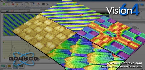
| Vision64™ |
 |
| – Intuitive Vision64™ user interface workflow simplifies operation |
| – Monitor uniformity of large area as opposed to single profile |
| – Multiple measurement parameters and data filtering options with analyzer recipes |
| – Data base analysis of multiple data sets |
| – Setup controls organized in a single window with logical workflow |
| – Fast, simple set up of multi-scan, multi-site recipes and data base analysis |
| – Up to 40% faster data collection for long scans and large 3D maps (option) |
Thông tin bổ sung
| Hãng sản xuất | Bruker Nano |
|---|---|
| Xuất xứ | Đức |
| Loại | Thủ công |