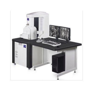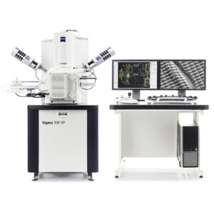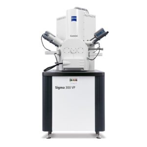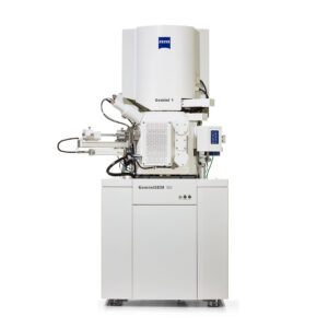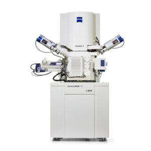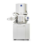
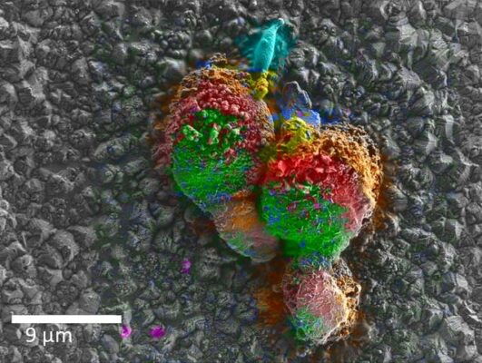
ZEISS GeminiSEM 560
- Mô tả
- Thông tin bổ sung
Mô tả
ĐIỂM NỔI BẬT
The New Standard in Surface Imaging
+ GeminiSEM 560 raises the bar for surface-sensitive, distortion-free, high resolution imaging and lets you image below 1 kV easily.
+ Magnetic field-free imaging of samples with sub 1 nm resolution below 1 kV – without the need for sample biasing or monochromation is enabled by Gemini 3 which includes the Nano-twin lens and the new electron optical engine Smart Autopilot.
+ Achieve images of non-conducting, vacuum- sensitive material with a new variable pressure mode and detection system: ensure fast results and preserve features by bringing vacuum-sensitive specimens into the chamber through the new Gentle Airlock in VP mode.
+ Analyze delicate samples with ease by leveraging the new, large chamber with dual EDS ports. Produce fast, shadow-free mapping ensured by an optimum detector solid angle.
Expert Knowledge Integrated
+ Imaging of challenging samples is now accelerated by the new electron optical engine Smart Autopilot.
+ Perform easy sample navigation by leveraging the greatly increased system’s field of view.
Smart Autopilot lets you save time while making lengthy alignments obsolete: the engine drives the electron optics to provide magnifications from less than 1× up to 500kx, taking care of alignment, calibration and focus along the way.
+ Smart Autopilot includes a new patented parallax autofocus and a new auto-wobble that provide you with clear, crisp images within seconds.
+ Python scripting is able to use these features in automated workflows such as 3D STEM tomography.
Experience Unique Contrast
+ Finding the sweet spot in your working conditions means that you’ve selected exactly the right combination of parameters to achieve the perfect image: the trick is finding it.
+ Gemini column technology with its magnetic field-free imaging and its new Gemini 3 column enables you to find these sweet spots and discover new information from your sample.
+ Magnetic contrast imaging is easy for GeminiSEM 560 with a magnetic field on the sample of less than 2 mT.
+ Perform energy spectroscopic imaging with the energy-selective Inlens back-scatter detector while simultaneously incorporating electron angular spectroscopic imaging, with the annular backscatter detector.
+ Bring all of your data together with ZEN Connect to segment and report on your findings with ease.
| ‘- Độ phân giải: | 0,4 nm @ 30 kV (STEM), 0,5 nm @ 15 kV, 0,7 nm @ 1 kV TD, 0,8 nm @ 1 kV, 1,0 nm @ 500 V |
| – Độ phân giải Inlens BSE : | 1.0 nm @ 1 kV. |
| – Độ phân giải ở chế độ NanoVP (30 Pa): | 1,4 nm @ 3 kV, 1,0 nm @ 15 kV |
| – Dòng điện thăm dò: | 3 pA – 20 nA (cũng có cấu hình 100 nA) |
| – Trường nhìn tối đa ở chế độ phân giải cao: | 1,6 mm ở 1 kV và WD = 7 mm |
| – Trường nhìn tối đa ở chế độ tổng quan: | 5,6 mm ở 15 kV và WD = 8,5 m, 130 mm ở cực đại. WD (khoảng 50 mm). |
| – Độ phóng đại: | 1 – 2.000.000 |
ZEISS GeminiSEM 560 với Electron Optics Gemini 3
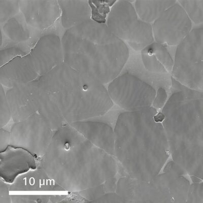
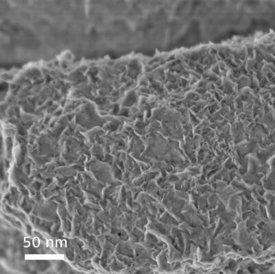
– Phân tích đặc tính bề mặt nhạy cảm ở cấp độ nanomet
– Gemini 3 với ống kính Nano-twin & Điều khiển tự động thông minh
– Cho hình ảnh tương phản độc đáo
Đang cập nhập…
Khoa học Vật liệu
+ Khoa học nano & vật liệu nano
+ Vật liệu năng lượng
+ Vật liệu sinh học, Polyme và Chất xúc tác
Ngành công nghiệp
+ Giải pháp kính hiển vi cho ngành công nghiệp
Điện tử và bán dẫn
+ Phân tích sai hỏng và thiết kế thiết bị bán dẫn
Khoa học đời sống
+ Đặc trưng của cấu trúc liên kết
+ Chụp ảnh các mẫu nhạy cảm, không dẫn điện.
Đang cập nhập…
| ZEN Connect: sắp xếp và căn chỉnh dữ liệu hình ảnh trong không gian làm việc tương quan |
| ZEN Connect 2D Add on: quy trình làm việc 2D tương quan tự động |
| ZEN Automated Imaging: Điều chỉnh hình ảnh SEM trong không gian làm việc của ZEN Connect |
| ZEN Intellesis: phân đoạn hình ảnh dựa machine learning |
| ZEN Data Storage: Có thể truy cập vào cơ sở dữ liệu trung tâm |
| 3DSM (mô phỏng bề mặt 3 chiều): mô phỏng bề mặt ba chiều theo thời gian thực. |
Thông tin bổ sung
| Hãng sản xuất | Zeiss |
|---|---|
| Xuất xứ | Đức |
| Loại | Bán tự động |