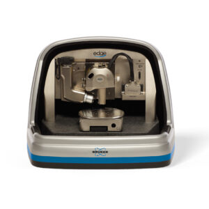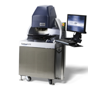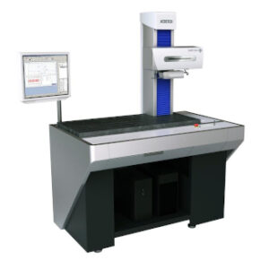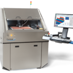
3D optical profilometer ContourSP
Incorporating over ten years of packaging optical characterization expertise, the ContourSP Large Panel Metrology System more than doubles the measurement throughput of high-density interconnect PCB (HDI-PCB) substrates over previous-generation WLI instruments. The system is specifically designed to measure each layer of the PCB panels during manufacturing, and incorporates a host of advanced features that deliver utmost production performance, convenience, reliability, and throughput for the semiconductor packaging industry. The gauge-capable ContourSP utilizes an intuitive production interface that offers fast and easy fiducial alignment with configurable user input.
- Mô tả
- Thông tin bổ sung
Mô tả
HIGHLIGHTS
Comprehensive industrial metrology
Enables rapid, high-precision PCB production control.
Unique system features
Assure highest yield, maximum uptime, and lowest cost per panel.
Highest throughput
Delivers 2x faster data without compromising accuracy.
| – Measurement Capability | Fully automated, non-contact, high-throughput, 3D HDI/PCB surface characterization; analysis library: Ra roughness, trace, via, pad clearance, dimple, anchor, overlay, soldermask, including via analysis for fiber-reinforced PCBs and thick film |
| – Advanced Functions: | Full- and semiautomatic remeasure functions; easy-to-use production mode with built-in databasing and pass/fail for any parameter optional stitching, MATLAB®/TCPIP, thick film, SureVision; optional COGNEX vision/recognition system; FixSure™ custom fixture designs for panels with up to 6mm warpage/bow |
| – Computer System | Advanced multi-core Intel processor PC with dual RAID1 drives; keyboard, mouse, joystick box for XY axis and Z focus control; 23 in. flat panel monitor mounted on Ergotron® support unit |
| – Field of View Multipliers | Discreet zoom lenses; 1X included; optional 0.55X, 0.75X, 1.5X, 2X |
| – Objectives | 2.5X, 5X, 10X, 20X, 50X for magnifications from 0.75X to 100X |
| – Lens Mounting | Quick-release motorized 5-position turret with automatic position sensing; optional quick-release single-objective adapter |
| – Vertical Measure Range | 0.1nm to 10mm standard |
| – Vertical Resolution | <0.1nm |
| – Vertical Scan Speed | User selectable up to 80μm/sec |
| – Lateral Spatial Sampling | 0.1 to 13.2μm (≤160nm with large-format camera) |
| – Optical Resolution | 0.55μm min. (based on Sparrow Criteria at 600nm) |
| – Field-of-View | 8.45mm to 0.05mm (10.8mm x 8.1mm max. with large format camera); optional stitching for larger FOVs |
| – Step Height | 0.6% accuracy; <0.1% to 100% at 1s repeatability |
| – Footprint | 163cm H x 143cm D x 115cm W (64in. H x 56in. D x 45in. W) |
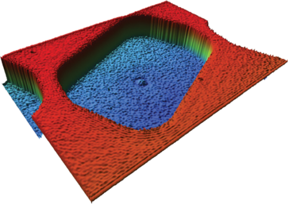
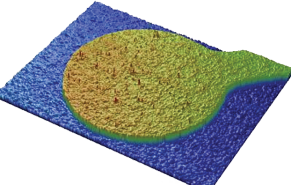
Unmatched Accuracy
With its new vibration-tolerant system design and patented Wyko Vertical Scanning Interferometry (VSI) imaging, the gauge-capable ContourSP system performs extremely accurate 3D critical dimensional (CD) measurements in nanometer resolution. This ability combined with extensive automation allows ContourSP to multitask as both a powerful surface texture metrology instrument as well as an easy-to-use defect inspection tool.
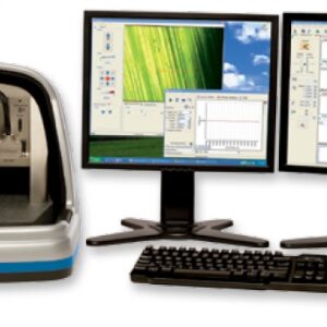
Streamlined Operation and Analysis
The ContourSP intuitive production interface offers fast and easy fiducial alignment with configurable user input. In addition to pass/fail information, users can now select detailed parameter results for display on the summary screen. Vision64 software provides full access control for engineers, technicians and operators with easy coordinate file import capability, guaranteeing system-to-system recipe portability and fast file creation.
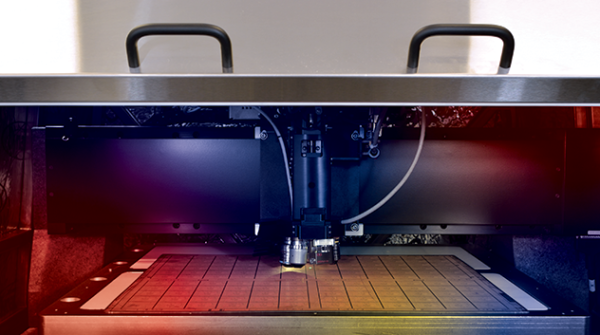
Large Measurable Area Tailored to Panel Metrology
The system utilizes Bruker’s revolutionary gantry-based design and integrated workstation to support up to 600×600 millimeter samples in a highly compact footprint. Software designed specifically for production panel metrology helps manufacturing engineers and operators to take the fullest advantage of the unique optical profiling features with dynamic signal segmentation, remeasure functionality, topography scanning to compensate for wafer bow, coordinate file import, ESD, panel ID reading, and pattern recognition.
Updating…..
Key application areas:
•Automotive/Aerospace
•Data Storage
•Solar
•MEMS
•Semiconductor
•LED, Optics
•Medical
•Precision Machining/Tribology
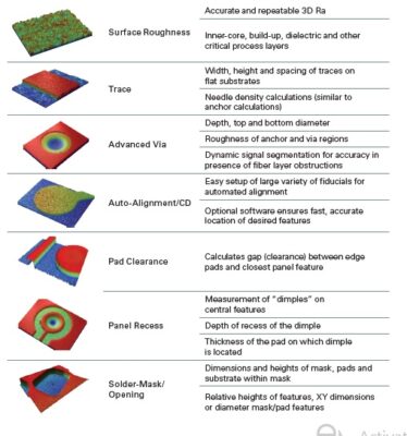
Industry’s Most Comprehensive Analyses:
+Surface Roughness
+Trace
+Advanced Via
+Auto-Alignment/CD
+Pad Clearance
+Panel Recess
+Solder-Mask/Opening
Updating…
Comprehensive PCB-HDI-MCM panel and thick film analysis suite; Vision64 3D optical measurement and analysis software;
Microsoft® Windows 7® 64-bit O/S
Thông tin bổ sung
| Hãng sản xuất | Bruker Nano |
|---|---|
| Xuất xứ | Đức |
| Loại | Tự động |